CLICK HERE to download TDA7294 Amplifier circuit diagram
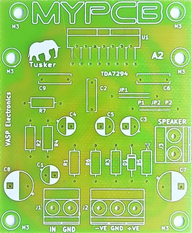
The circuit is quite simple, main job of amplification is done by ic U1 and rest are the supporting components.
Input signal is fed to pin no.3 (Non Inverting Input) through R1 & C2. R7 defines the input impedance.
R2 & R4 connected to Pin no.2 (Inverting input) set the closed loop gain. Changing the value of any one these resistors will change the gain of the amplifier.
Pin no.9 (Stand by) - R6 keeps ic U1 in active mode by providing positve voltage.
Pin no. 7, 13 are positive supply, Pin no. 8, 15 are negative supply and 1, 4 are ground pins. Pin no.14 is the output pin.
Mute Function - Pin no.10 (Mute) is connected to JP2. To use the mute function replace JP2 with a switch.
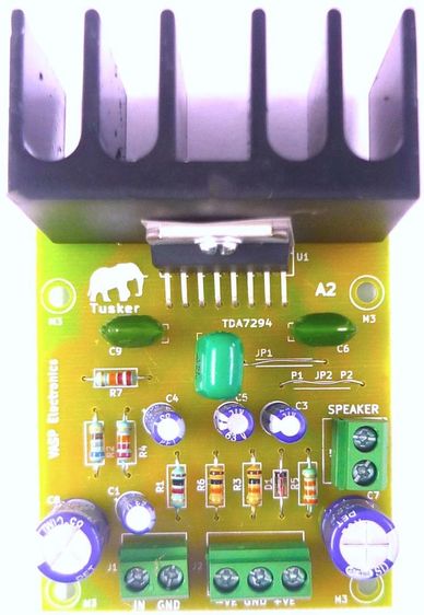
Metal Tab of ic U1 is connected to negative supply internally, so proper insulation is necessary when fitting ic U1 on heatsink.